
Dilution refrigerator

Top-loading, top-shelf cryo-free dilution refrigerator, manufactured by Leiden Cryogenics. It provides a base temperature of about 7 mK for our experiments. It's equipped with a 2D vector magnet capable of applying a magnetic induction of 9 T along the principal axis, and 3 T in any direction in a vertical plane. Two samples can be simultaneously cooled down in the fridge using the top-loading probes, the dilution unit provides a cooling power of 100 uW at 100 mK.
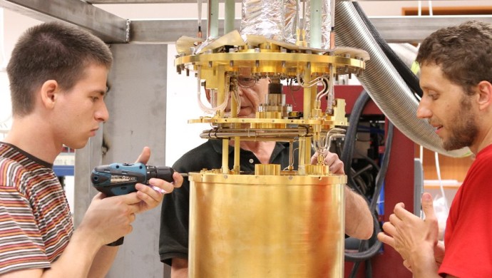
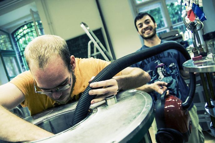
Working hard, from left to right: Gergő, Makita, Sándor, fridge, Szabolcs. Assembling (or disassembling?) the fridge, inside of the inner vacuum chamber revealed.
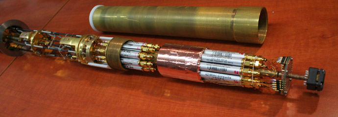
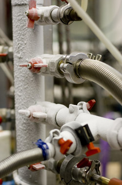
Cold finger of the main probe, cap removed exposing the low-pass filters.
Spooky effect at a distance (vector magnet in operation).
Installation of the dilfridge, time lapse movie.
Oxford cryostat

The Oxford cryostat has a magnet capable of reaching 8 T magnetic induction. It can be equipped with a Variable Temperature Insert (VTI) with a needle valve, enabling us to perform measurements at as low as 1.5 K. Though accomodating only a single probe, loading and cooling down a sample takes less than two hours, making this cryo ideal for measuring, or simply testing various devices that don't require ultra low temperature, in a magnetic field.
A still-cold probe (left), and a part of the helium gas recovery system (right) closest to the cryostat during refill with liquid He.

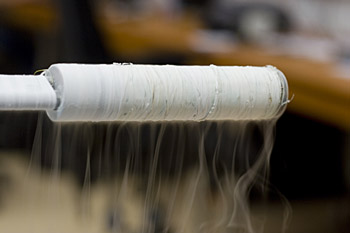
In the summertime, with a cold VTI...
A cryostat by Cryogenic Limited, refillable with liquid He, similarly to the Oxford. The superconducting magnet's top field is 15 T at 4 K, however, using the Lambda-plate for cooling down further, the field can be set to as much as 17 T.
Vanessa, the transfer optical microscope
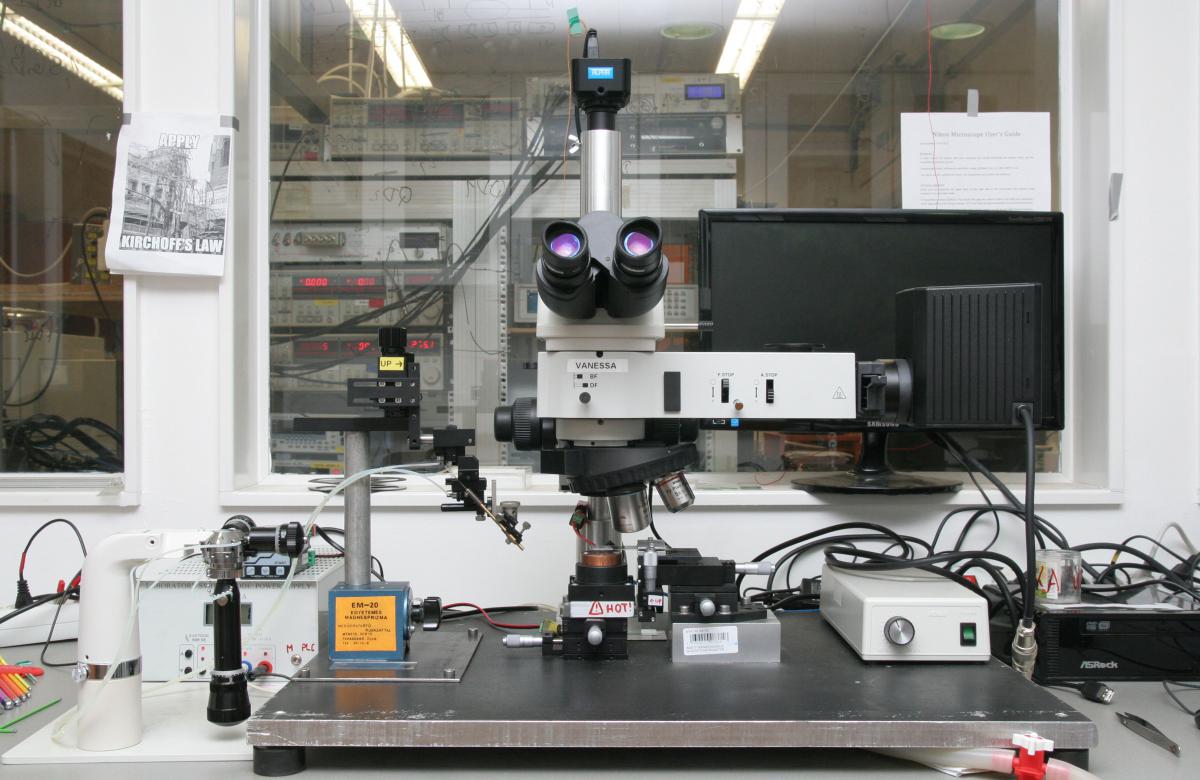
This is an optical microscope-assisted transfer system using two separate ThorLabs micromanipulator set and a three-axis hanging joystick oil-hydraulic micromanipulator. The optical microscope focuses via a moving upper part, while the steady sample holder manipulators enable precise positioning and reliable bottom-up assembly processes like dry-stacking assembly for graphene and other types of heterostructures or nanowire positioning for cooper-pair-splitter circuits. The sample is hold by vacuum at the desired position.

The manipulator-driven stage can be heated up to 150 degrees Celsius using a PID controller with thermometer feedback and a power supply.

The Narishige oil-hydraulic joystick manipulator driving a glass needle. The tip of the needle can be as small as 100 nm.

This is an example of a sharp glass needle tip.
This is an example of the manipulation of an InSb nanowire by the glass needle in darkfield illumination. With the joystick-driven manipulator it is easy and fast to rotate and straighten the nanowire in the desired angle.

This picture shows the backside of the complicated stage (heating, vacuum and thermometer connections). The ThorLabs manipulators are used for dry-stacking assembly of a graphene heterostructure.
María Luisa, the standard optical microscope
Optical microscope with lenses between 5x and 100x, brightfield & darkfield illumination; equipped with a moving stage.
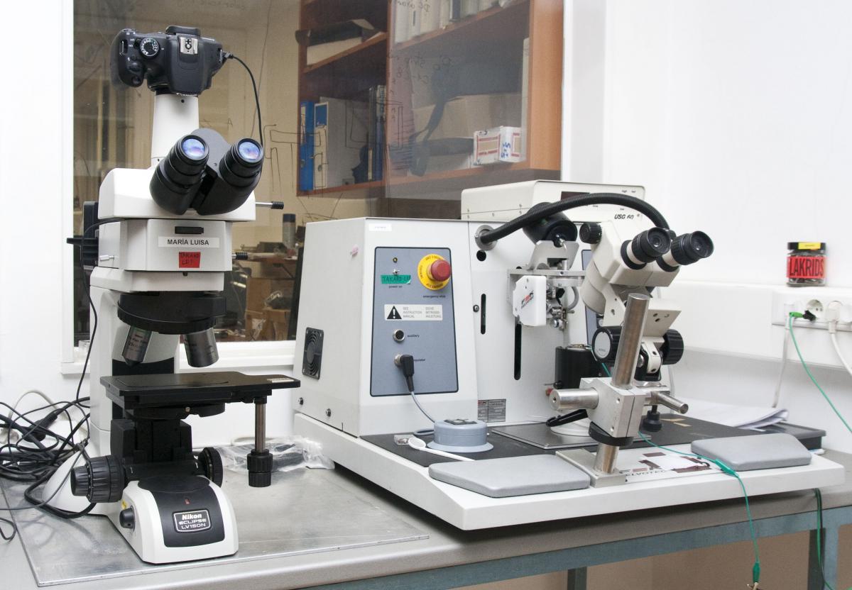
María Luisa with the bonder.

This image shows the working principle of the darkfield illumination: the light is lead down to the sample in the side of the lens and is shone in a very low angle on the sample. Thus, all the obstacles protuberating of the substrate plane are illuminated. An application of the darkfield illumination is shown above, at the Vanessa transfer microscope.
The probe station
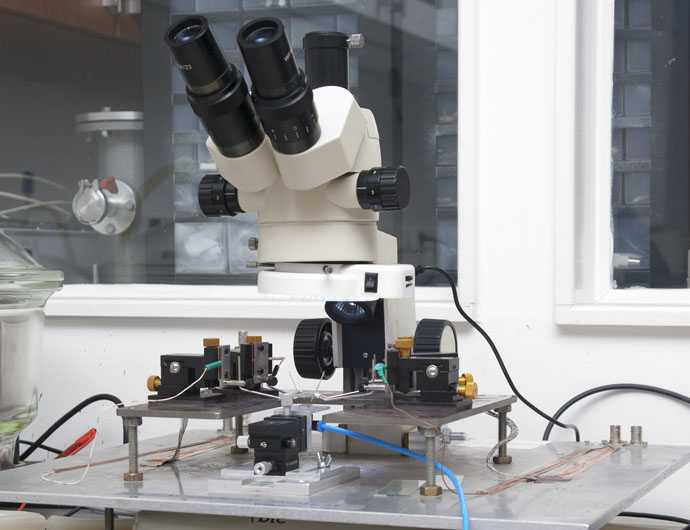
Works with metal probe needles and has corresponding electrical connections. Using the optical microscope fast and easy measurements can be done in the intermediate setps of the sample fabrication.
Bonder

Wedge bonder from F&K Delvotec. We use a 25 um thin aluminum wire to make electrical connections between the circuits on the silicon wafer and the chip socket. The electrical joint is created by gently pressing the wire against the surface and applying a lateral ultrasonic vibration.

Close-up of the wedge and a sample.
UV Ozone cleaner

It cleans stuff.
Joint Nanolitography Lab of MFA and Dep. of Physics BME
This clean room laboratory is located at the KFKI physics facility and serves general lithography purposes for several research group.
Raith 150two nanolithography system

This system is the propriety of MFA. This is a professional lithography system of 10 nm order of magnitude accuracy and several advanced lithography features e.g. stitching field patterning, automatic focus correction, different kinds of drift compensation, FBMS (fixed beam -- moving stage) patterning method.
AJA
This device is the propriety of the BME Nanoelectronics group and is used widely.

Another example of the darkfield illumination:)
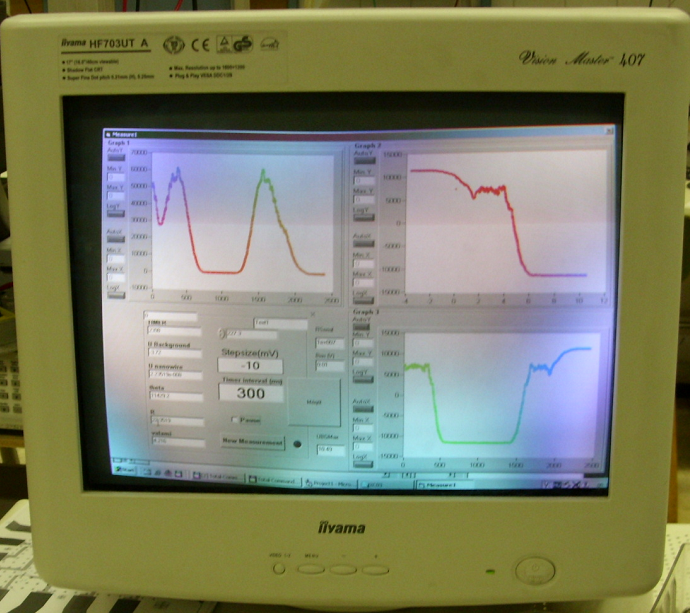
Before LCD monitors: a CRT monitor about 2 meters from an ongoing quantum Hall measurement on graphene in a cryostat, at around 10 T magnetic field inside.

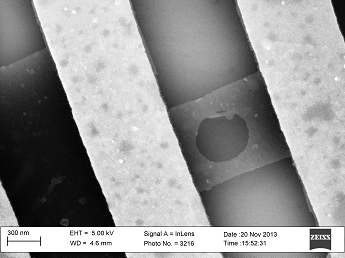
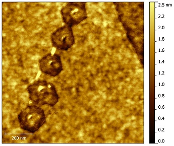
Left: optical photo of graphite on SiO2 with thicknesses up to about 80 nm (from dark blue to yellow). Right: SEM image of suspended graphene with etched hole (made in Basel).

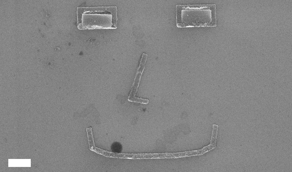
Left: AFM scan of anisotropically etched nanoribbons (lighter strips). Right: SEM image of plasma-etched nanoribbons (darkest strips) with metallic contacts (light gray) fabricated using electron-beam lithography.

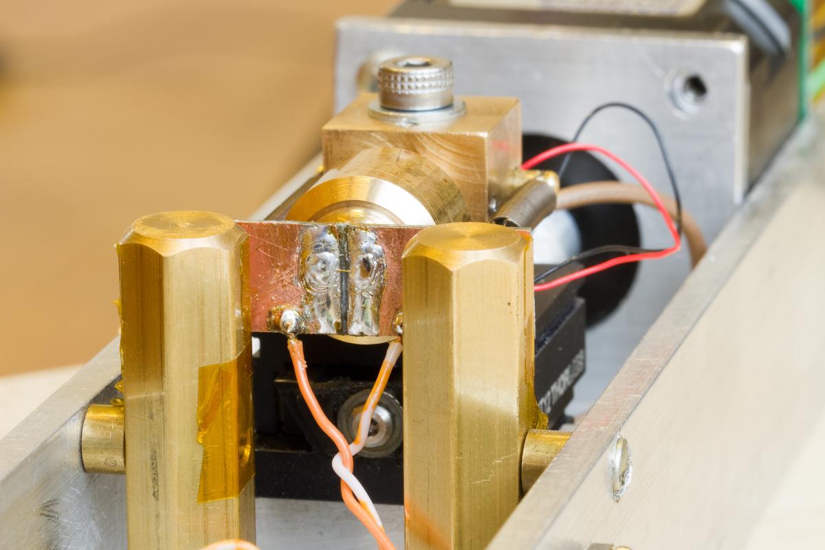
Low temperature MCBJ sample holder with heated tube and the EM shutter and molecular dosing hole.
MCBJ device for educational purposes