Our central research objective is to establish and study novel device structures, where the characteristic size of the active region is close to atomic dimensions.
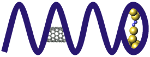
Our research group has long tradition in investigating single-atom and single-molecule conduction using the mechanically controllable break junction (MCBJ) technique. By mounting a metallic wire on the top of a bending beam and breaking the wire by the precise control of the bending one can investigate the final stage of the rupture, when the current flows through a single atom in the narrowest cross section (panel a). After the disconnection of the single-atom contact a sub-nanometer scale variable gap is established at the apex of the broken wire providing an ideal platform for contacting single molecules. Using this method several types of measurements can be performed, like the identification of single-atom or single molecule conductances by conductance histograms, the study of the transmission channels by superconducting subgap spectroscopy, the investigation of inelastic excitations by point-contact spectroscopy, or the study of junction evolution dynamics by advanced statistical methods (panels b-h).
We have extended our experimental capabilities by building self-designed scanning tunneling microscope (STM) setups operating either at room temperature or at cryogenic circumstances. Whereas the MCBJ technique has superior stability to an STM, the STM setups enable the study of atomic-scale objects between two different electrode materials. Using this heterojunction geometry we focus on the study of atomic scale resistive switching memories (panel a), and the investigation of local, nanoscale spin polarization by Andreev spectroscopy (panel b).
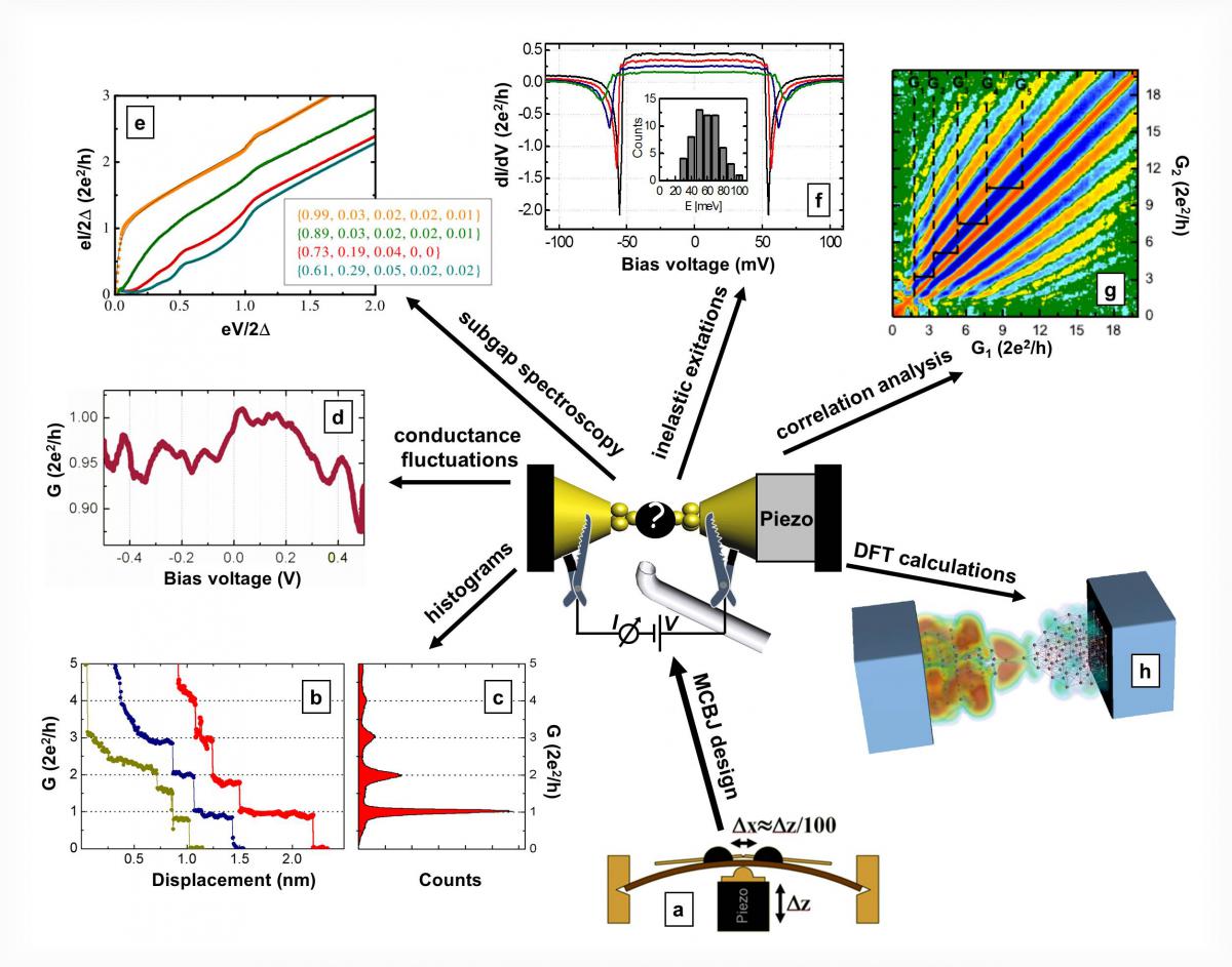
As a third platform we study nanocircuits predifiend by electron beam lithography, and thinned further to atomic dimensions by electromigration or electroburning techniques (panel c).

Some selected results:
Investigation of ultra-small resistive switching memories

We have investigated several memristive systems (including Ag2S, AgI, Nb2O5, and SiO2) with the common goal of studying resistive switching phenomena at ultra-small, close-to-atomic-scale dimensions. Along these studies we have demonstrated the crossover from a stochastic single-atomic switch to nanoscale resistive memory device; we have studied the size of the conducting channels in the active volume of the resistive switching junction by superconducting Andreev spectroscopy; we have investigated the temporal dynamics of the switching also demonstrating transitions due to sub-nanosecond pulses; we have highlighted the role of the selfheating and the local geometrical asymmetry of the junction in the switching process, we have demonstrated the universal ballistic to diffusive crossover of the 1/f type noise in silver nanowire based memristors, and we have identified the multiple physical time-scales and the dead time rule in graphene-SiO2-graphene resistive switching devices.
B. Sánta, Z. Balogh, A. Gubicza, L. Pósa, D. Krisztián, G. Mihály, M. Csontos, A. Halbritter, NANOSCALE (2019)
D. Molnár, T.N. Török, B. Sánta, A. Gubicza, A. Magyarkuti, R. Hauert, G. Kiss, A. Halbritter, M. Csontos, NANOSCALE (2018)
L. Pósa, M. El Abbassi, P. Makk, B. Sánta, C. Nef, M. Csontos, M. Calame, A. Halbritter, NANO LETTERS (2017)
A. Gubicza, D. Zs. Manrique, L. Pósa, C. J. Lambert, G. Mihály, M. Csontos, A. Halbritter, SCIENTIFIC REPORTS (2016)
A. Gubicza, M. Csontos, A. Halbritter, G. Mihály, NANOSCALE (2015)
A. Gubicza, M. Csontos, A. Halbritter, G. Mihály, NANOSCALE (2015)
A. Geresdi, M. Csontos, A. Gubicza, A. Halbritter, G. Mihály, NANOSCALE (2014)
A. Geresdi, A. Halbritter, E. Szilágyi, G. Mihály, MATERIALS RESEARCH SOCIETY SYMPOSIUM PROCEEDINGS (2011)
A. Geresdi, A. Halbritter, A. Gyenis, P. Makk, G. Mihaly, NANOSCALE (2011)
Nanometer-sized gaps in CVD graphene
In collaboration with the group of M. Calame at the University of Basel we demonstrated the controlled and reproducible fabrication of sub-5 nm wide gaps in single-layer graphene electrodes. The process is implemented for graphene grown via chemical vapor deposition using an electroburning process at room temperature and in vacuum. A yield of over 95% for the gap formation is obtained. This approach allows producing single-layer graphene electrodes for molecular electronics at a large scale.
M. El Abbassi, L. Posa, P. Makk, C. Nef, K. Thodkar, A. Halbritter, M. Calame, NANOSCALE (2017)
C. Nef, L. Pósa, P. Makk, W. Fu, A. Halbritter, C. Schönenberger, M. Calame, NANOSCALE (2014)
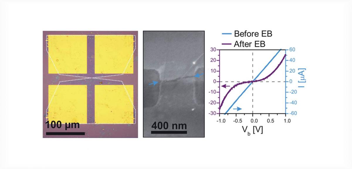
Advanced statistical analysis of atomic and single-molecule junction conductance
We have developed novel statistical methods for the advanced analysis of single-atom and single-molecule break junction data including the cross-correlation analysis of conductance traces, the investigation of temporal correlations and opening-closing correlations, and the classification of the typical single-atom and single molecule features by neural network algorithms. These methods are capable of resolving fine ingredients of the nanocontact formation dynamics, which are completely hidden in traditional conductance histograms, including the identification of precursor molecular configurations, the detailed understanding of molecule decorated atomic chain formation processes, the recognition of structural memory effects, and the efficient classification of the relevant features in the conductance traces.
K.P. Lauritzen, A. Magyarkuti, Z. Balogh, A. Halbritter, G.C. Solomon, JOURNAL OF CHEMICAL PHYSICS (2018)
A. Magyarkuti, O. Adak, A. Halbritter, L. Venkataraman, NANOSCALE (2018)
A. Magyarkuti, K.P. Lauritzen, Z. Balogh, A. Nyáry, G. Mészáros, P. Makk, G.C. Solomon, A. Halbritter, JOURNAL OF CHEMICAL PHYSICS (2017)
Z. Balogh, P. Makk, A. Halbritter, BEILSTEIN JOURNAL OF NANOTECHNOLOGY (2015)
Z. Balogh, D. Visontai, P. Makk, K. Gillemot, L. Oroszlány, L. Pósa, C. Lambert, A. Halbritter, NANOSCALE (2014)
SV. Aradhya, M. Frei, A. Halbritter, L. Venkataraman, ACS NANO, (2013)
P. Makk, Z. Balogh, S. Csonka, A. Halbritter, NANOSCALE (2012)
P. Makk, D. Tomaszewski,J. Martinek, Z. Balogh, S. Csonka, M. Wawrzyniak, M. Frei, L. Venkataraman, A. Halbritter, ACS NANO (2012)
A. Halbritter, P. Makk, S. Mackowiak, S. Csonka, M. Wawrzyniak, J. Martinek, PHYSICAL REVIEW LETTERS (2010)
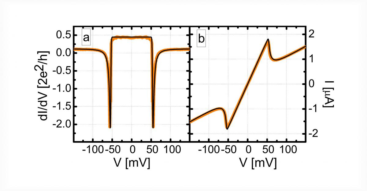
Investigation of transmission channels by subgap spectroscopy
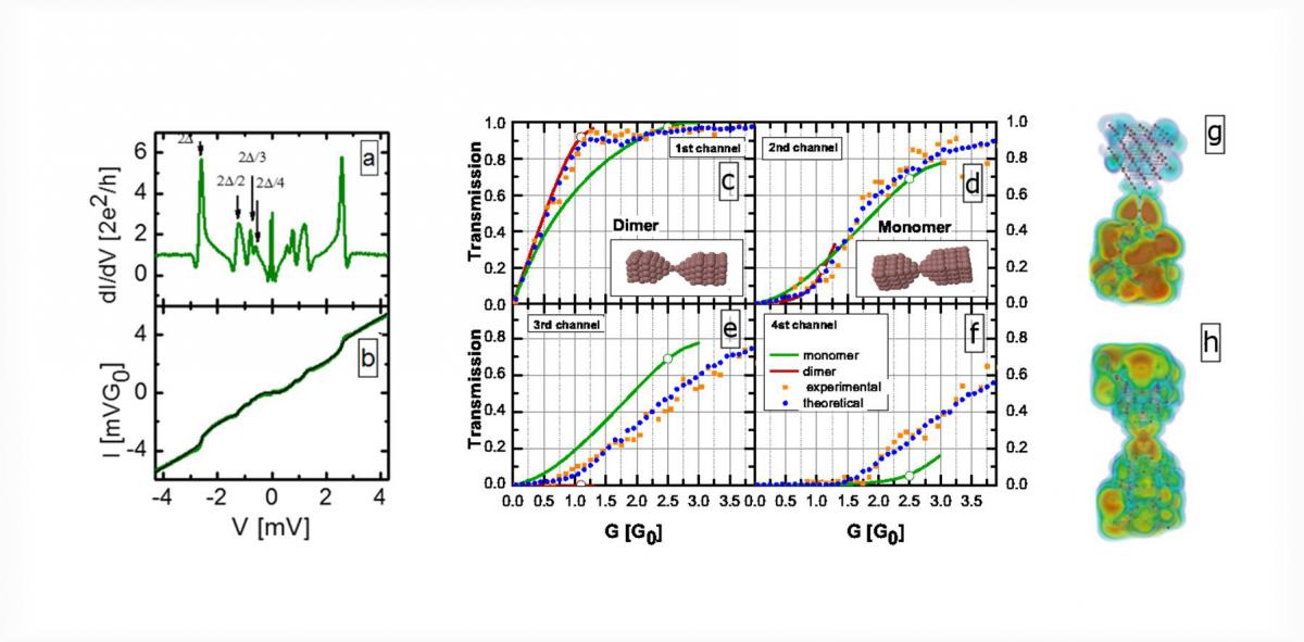
We have investigated the opening of conductance channels in atomic and molecular contacts by superconducting subgap method. Subgap structure measurements give a unique opportunity for the full determination of transmission probabilities for all the conductance channels, and the evolution of the channel transmission as a function of total conductance is characteristic of the studied system, providing significantly more information than the conductance histogram alone.
P. Makk, D. Visontai, L. Oroszlany, DZ. Manrique, S. Csonka, J. Cserti, C. Lambert, A. Halbritter, PHYSICAL REVIEW LETTERS (2011)
P. Makk, S. Csonka, A. Halbritter, PHYSICAL REVIEW B CONDENSED MATTER AND MATERIALS PHYSICS (2008)
Measurement of local, nanoscale spin polarization

We investigated the local, nanoscale spin polarization by means of point contact Andreev reflection measurements, demonstrating that this method is capable of determining the spin diffusion length in ferromagnet/normal metal thin film structures. We have also demonstrated the presence of local magnetism well above the bulk Curie temperature of (In,Mn)Sb magnetic semiconductors.
A. Halbritter, A. Geresdi, G. Mihaly, FRONTIERS IN NANOSCIENCE AND NANOTECHNOLOGY (2016)
A. Geresdi, A. Halbritter, F. Tancziko, G. Mihaly, APPLIED PHYSICS LETTERS (2011)
A. Geresdi, A. Halbritter, M. Csontos, S. Csonka, G. Mihály, T. Wojtowicz, X Liu, B. Jankó, JK. Furdyna, PHYSICAL REVIEW B CONDENSED MATTER AND MATERIALS PHYSICS (2008)
Huge negative differential conductance
We have shown that I-V characteristics of molecular nanojunctions frequently show huge nonlinearities, even negative differential conductance due to the excitation of a strongly bound molecule to a large number of energetically similar loosely bound states.
A. Halbritter, P. Makk, S. Csonka, G. Mihály, PRB (2008)
A. Halbritter, L. Borda, A. Zawadowski, ADVANCES IN PHYSICS (2004)